 Lattice ECP5和ECP5-5G FPGA系列VIP处理器解决方案

lattice公司的ECP5/ECP5-5G FPGA系列提供了高性能特性如增强DSP架构,高速SERDES和高速源同步接口,采用40nm技术,使得器件非常适合于量大高速和低成本的应用.器件的查找表(LUT)高达48K逻辑单元,支持多达365个用户I/O,提供多达156个18x18乘法器和各种并行I/O标准,采用可配置SRAM逻辑技术,提供基于LUT的逻辑,分布式和嵌入式存储器,锁相环(PLL),延迟锁定环(DLL),支持预制源同步I/O,增强sysDSP slices和高挡配置,包括加密和双引导功能.本文介绍了ECP5和ECP5-5G FPGA系列主要特性,LFE5UM/LFE5UM5G-85器件简化框图以及ECP5 VIP 处理器板主要特性,框图,电路图和材料清单.
The ECP5/ECP5-5G family of FPGA devices is optimized to deliver high performance features such as an enhanced DSP architecture, high speed SERDES (Serializer/Deserializer), and high speed source synchronous interfaces, in an economical FPGA fabric. This combination is achieved through advances in device architecture and the use of 40 nm technology making the devices suitable for high-volume, high-speed, and low-cost applications.
The ECP5/ECP5-5G device family covers look-up-table (LUT) capacity to 84K logic elements and supports up to 365 user I/Os. The ECP5/ECP5-5G device family also offers up to 156 18 x 18 multipliers and a wide range of parallel I/O standards.
The ECP5/ECP5-5G FPGA fabric is optimized high performance with low power and low cost in mind. The ECP5/ ECP5-5G devices utilize reconfigurable SRAM logic technology and provide popular building blocks such as LUT-based logic, distributed and embedded memory, Phase-Locked Loops (PLLs), Delay-Locked Loops (DLLs), pre-engineered source synchronous I/O support, enhanced sysDSP slices and advanced configuration support, including encryption and dual-boot capabilities.
The pre-engineered source synchronous logic implemented in the ECP5/ECP5-5G device family supports a broad range of interface standards including DDR2/3, LPDDR2/3, XGMII, and 7:1 LVDS.
The ECP5/ECP5-5G device family also features high speed SERDES with dedicated Physical Coding Sublayer (PCS) functions. High jitter tolerance and low transmit jitter allow the SERDES plus PCS blocks to be configured to support an array of popular data protocols including PCI Express, Ethernet (XAUI, GbE, and SGMII) and CPRI. Transmit De-emphasis with pre- and post-cursors, and Receive Equalization settings make the SERDES suitable for transmission and reception over various forms of media.
The ECP5/ECP5-5G devices also provide flexible, reliable and secure configuration options, such as dual-boot capability, bit-stream encryption, and TransFR field upgrade features.
ECP5-5G family devices have made some enhancement in the SERDES compared to ECP5UM devices. These enhancements increase the performance of the SERDES to up to 5 Gb/s data rate. The ECP5-5G family devices are pin-to-pin compatible with the ECP5UM devices. These allows a migration path for users to port designs from ECP5UM to ECP5-5G devices to get higher performance.
The Lattice Diamond? design software allows large complex designs to be efficiently implemented using the ECP5/ECP5-5G FPGA family. Synthesis library support for ECP5/ECP5-5G devices is available for popular logic synthesis tools. The Diamond tools use the synthesis tool output along with the constraints from its floor planning tools to place and route the design in the ECP5/ECP5-5G device. The tools extract the timing from the routing and back-annotate it into the design for timing verification.
Lattice provides many pre-engineered IP (Intellectual Property) modules for the ECP5/ECP5-5G family. By using these configurable soft core IPs as standardized blocks, designers are free to concentrate on the unique aspects of their design, increasing their productivity.
Each ECP5/ECP5-5G device contains an array of logic blocks surrounded by Programmable I/O Cells (PIC). Interspersed between the rows of logic blocks are rows of sysMEM? Embedded Block RAM (EBR) and rows of sysDSP? Digital Signal Processing slices, as shown in Figure 2.1 on page 13. The LFE5-85 devices have three rows of DSP slices, the LFE5-45 devices have two rows, and both LFE5-25 and LFE5-12 devices have one. In addition, the LFE5UM/LFE5UM5G devices contain SERDES Duals on the bottom of the device.
The Programmable Functional Unit (PFU) contains the building blocks for logic, arithmetic, RAM and ROM functions. The PFU block is optimized for flexibility, allowing complex designs to be implemented quickly and efficiently. Logic Blocks are arranged in a two-dimensional array.
The ECP5/ECP5-5G devices contain one or more rows of sysMEM EBR blocks. sysMEM EBRs are large, dedicated 18 Kb fast memory blocks. Each sysMEM block can be configured in a variety of depths and widths as RAM or ROM. In addition, ECP5/ECP5-5G devices contain up to three rows of DSP slices. Each DSP slice has multipliers and adder/accumulators, which are the building blocks for complex signal processing capabilities.
The ECP5 devices feature up to four embedded 3.2 Gb/s SERDES channels, and the ECP5-5G devices feature up to four embedded 5 Gb/s SERDES channels. Each SERDES channel contains independent 8b/10b encoding / decoding, polarity adjust and elastic buffer logic. Each group of two SERDES channels, along with its Physical Coding Sublayer (PCS) block, creates a dual DCU (Dual Channel Unit). The functionality of the SERDES/PCS duals can be controlled by SRAM cell settings during device configuration or by registers that are addressable during device operation. The registers in every dual can be programmed via the SERDES Client Interface (SCI). These DCUs (up to two) are located at the bottom of the devices.
Each PIC block encompasses two PIOs (PIO pairs) with their respective sysI/O buffers. The sysI/O buffers of the ECP5/ECP5-5G devices are arranged in seven banks (eight banks for LFE5-85 devices in caBGA756 and caBGA554 packages), allowing the implementation of a wide variety of I/O standards. One of these banks (Bank 8) is shared with the programming interfaces. Half of the PIO pairs on the left and right edges of the device can be configured as LVDS transmit pairs, and all pairs on left and right can be configured as LVDS receive pairs. The PIC logic in the left and right banks also includes pre-engineered support to aid in the implementation of high speed source synchronous standards such as XGMII, 7:1 LVDS, along with memory interfaces including DDR3 and LPDDR3.
The ECP5/ECP5-5G registers in PFU and sysI/O can be configured to be SET or RESET. After power up and the device is configured, it enters into user mode with these registers SET/RESET according to the configuration setting, allowing the device entering to a known state for predictable system function.
Other blocks provided include PLLs, DLLs and configuration functions. The ECP5/ECP5-5G architecture provides up to four Delay-Locked Loops (DLLs) and up to four Phase-Locked Loops (PLLs). The PLL and DLL blocks are located at the corners of each device.
The configuration block that supports features such as configuration bit-stream decryption, transparent updates and dual-boot support is located at the bottom of each device, to the left of the SERDES blocks. Every device in the ECP5/ECP5-5G family supports a sysCONFIG? ports located in that same corner, powered by Vccio8, allowing for serial or parallel device configuration.
In addition, every device in the family has a JTAG port. This family also provides an on-chip oscillator and soft error detect capability. The ECP5 devices use 1.1 V and ECP5UM5G devices use 1.2 V as their core voltage.
ECP5和ECP5-5G FPGA系列主要特性:
? Higher Logic Density for Increased System Integration
? 12K to 84K LUTs
? 197 to 365 user programmable I/Os
? Embedded SERDES
? 270 Mb/s, up to 3.2 Gb/s, SERDES interface(ECP5)
? 270 Mb/s, up to 5.0 Gb/s, SERDES interface (ECP5-5G)
? Supports eDP in RDR (1.62 Gb/s) and HDR (2.7 Gb/s)
? Up to four channels per device: PCI Express, Ethernet (1GbE, SGMII, XAUI), and CPRI sysDSP?
? Fullycascadable slice architecture
? 12 to 160 slices for high performance multiply and accumulate
? Powerful 54-bit ALU operations
? Time Division Multiplexing MAC Sharing
? Rounding and truncation
? Each slice supports
? Half 36 x 36, two 18 x 18 or four 9 x 9 multipliers
? Advanced 18 x 36 MAC and 18 x 18 Multiply-Multiply-Accumulate (MMAC) operations
? Flexible Memory Resources
? Up to 3.744 Mb sysMEM? Embedded Block RAM (EBR)
? 194K to 669K bits distributed RAM
? sysCLOCK Analog PLLs and DLLs
? Four DLLs and four PLLs in LFE5-45 and LFE5-85; two DLLs and two PLLs in LFE5-25 and LFE5-12
? Pre-Engineered Source Synchronous I/O
? DDR registers in I/O cells
? Dedicated read/write levelling functionality
? Dedicated gearing logic
? Source synchronous standards support
? ADC/DAC, 7:1 LVDS, XGMII
? High Speed ADC/DAC devices
? Dedicated DDR2/DDR3 and LPDDR2/LPDDR3 memory support with DQS logic, up to 800 Mb/s data-rate
? Programmable sysI/O? Buffer Supports Wide Range of Interfaces
? On-chip termination
? LVTTL and LVCMOS 33/25/18/15/12
? SSTL 18/15 I, II
? HSUL12
? LVDS, Bus-LVDS, LVPECL, RSDS, MLVDS
? subLVDS and SLVS, MIPI D-PHY input interfaces
? Flexible Device Configuration
? Shared bank for configuration I/Os
? SPI boot flash interface
? Dual-boot images supported
? Slave SPI
? TransFR? I/O for simple field updates
? Single Event Upset (SEU) Mitigation Support
? Soft Error Detect – Embedded hard macro
? Soft Error Correction – Without stopping user operation
? Soft Error Injection – Emulate SEU event to debug system error handling
? System Level Support
? IEEE 1149.1 and IEEE 1532 compliant
? Reveal Logic Analyzer
? On-chip oscillator for initialization and general use
? 1.1 V core power supply for ECP5, 1.2 V core power supply for ECP5UM5G
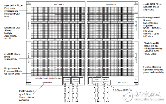
图1. LFE5UM/LFE5UM5G-85器件简化框图
ECP5 VIP 处理器板
This document describes the Lattice Semiconductor ECP5 VIP Processor Board which is a key component of Lattice’s Video Interface Platform (VIP) board interconnect. Lattice VIP boards can be interconnected to create solutions for MIPI? CSI-2/DSI, SERDES, LVDS and more.
The content of this user guide includes descriptions of onboard jumper settings, programming circuit, a complete set of schematics, and bill of materials for ECP5 VIP processor board.
ECP5 VIP 处理器板主要特性:
ECP5/5G
SERDES interface
Dual DDR3 interface
LVDS/MIPI Transmitter/Receiver interface
SPI flash configuration
General Purpose Input/Output
Programming Circuit
Mini-B USB connector to FTDI
FTDI to ECP5 using JTAG
FTDI to ispClock using JTAG
ispClock
SERDES reference clock generation interface
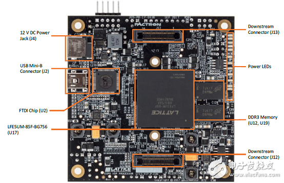
图2.ECP5 VIP 处理器板主要元件分布图(顶层)
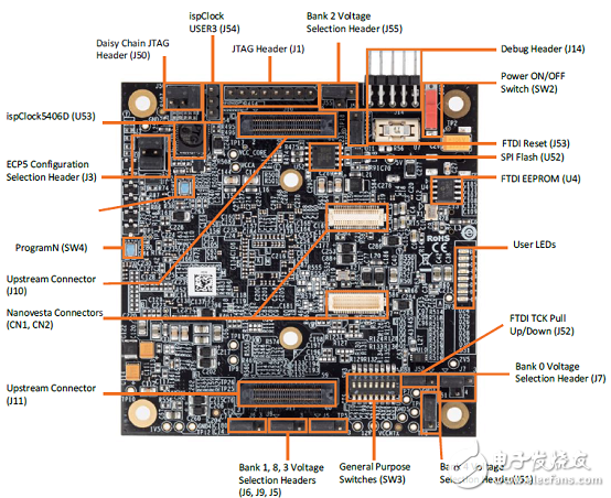
图3.ECP5 VIP 处理器板主要元件分布图(底层)
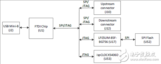
图4.ECP5 VIP 处理器板可编程框图
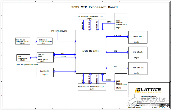
图5.ECP5 VIP 处理器板框图
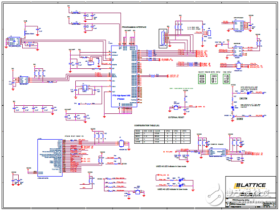
图6.ECP5 VIP 处理器板电路图(1):FTDI和编程接口
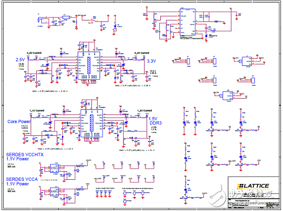
图7.ECP5 VIP 处理器板电路图(2):电源稳压器接口
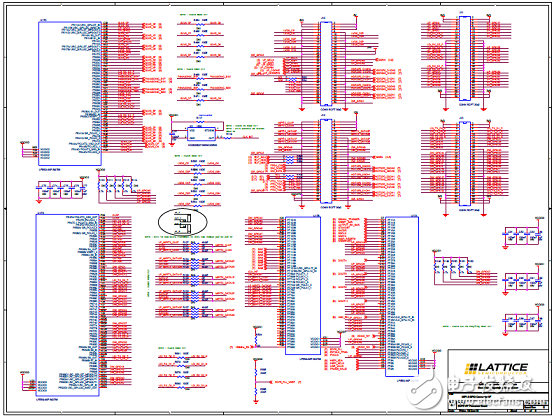
图8.ECP5 VIP 处理器板电路图(3):MIPI和GPIO连接器接口
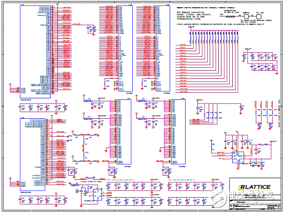
图9.ECP5 VIP 处理器板电路图(4):DDR3接口
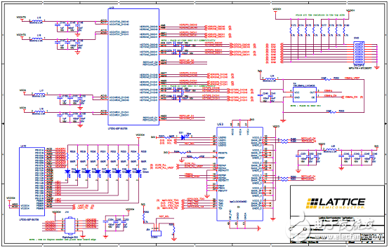
图10.ECP5 VIP 处理器板电路图(5):SERDES接口
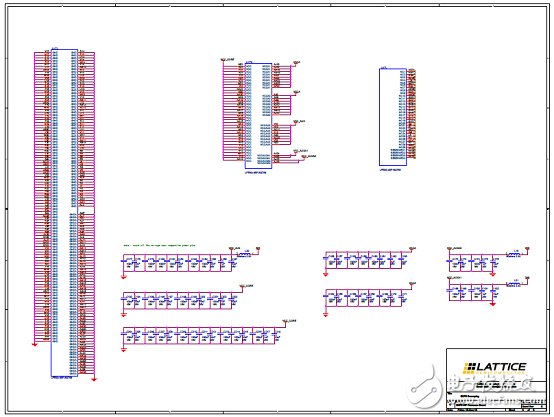
图11.ECP5 VIP 处理器板电路图(6):ECP5去耦
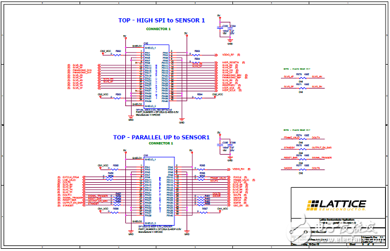
图12.ECP5 VIP 处理器板电路图(7):HISPI/CSI2连接器
ECP5 VIP 处理器板材料清单:
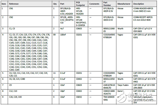
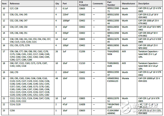
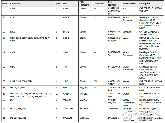
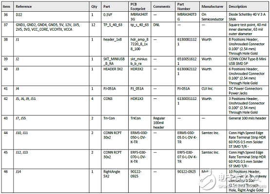
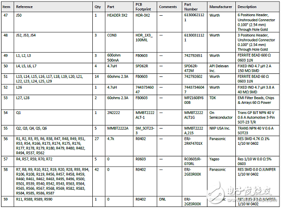
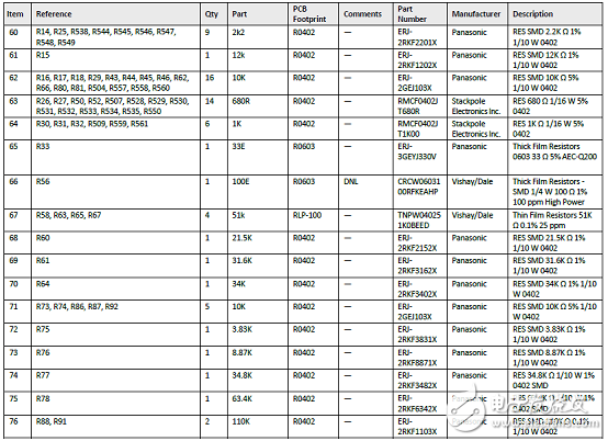
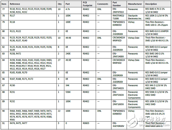
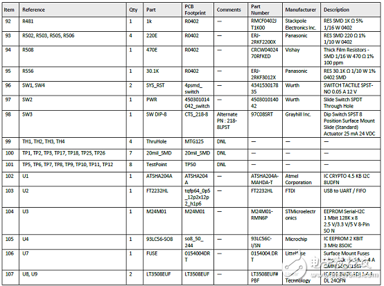
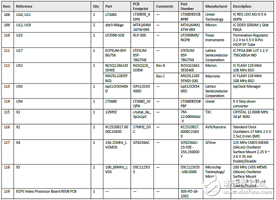
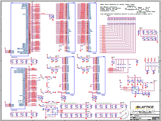
图13.ECP5 VIP 处理器板电路图:DDR3接口B版本
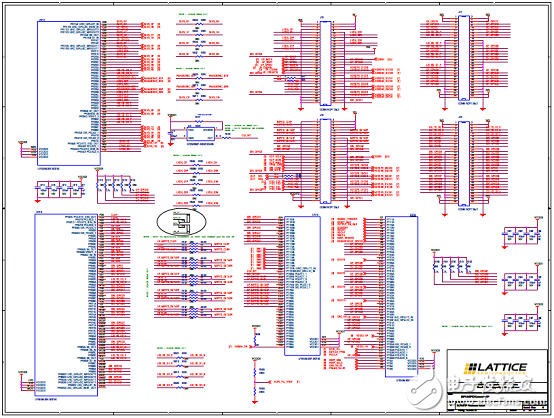
图14.ECP5 VIP 处理器板电路图:MIPI和GPIO连接器接口B版本
-
处理器
+关注
关注
68文章
19951浏览量
237374
发布评论请先 登录
开源Made with KiCad(134):Icepi Zero - 基于Lattice ECP5的便携FPGA开发板
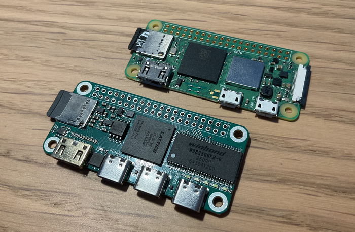
【开源分享】:开源小巧的FPGA开发板——Icepi Zero
广和通发布5G AI MiFi解决方案
华为双频MetaAAU系列解决方案推动5G-A规模落地
ECP信号会变高是什么原因导致的?
ADS6245EVM和Lattice ECP2/M接口演示用户指南

广和通发布5G RedCap MiFi解决方案

广和通发布5G RedCap MiFi解决方案
翱捷科技发布5G RedCap芯片平台ASR1903系列
Made with KiCad(八):Schoko FPGA电脑板


 工商网监
工商网监
评论