 赛普拉斯低成本高可靠嵌入式闪存技术

Outline
1. Charge-trap eNVMs at Cypress
2. SONOS
–Introduction
–Key Macro Specs
–High Reliability
3. eCT
–Introduction
–Key Macro Specs
–High Reliability
4. Embedded NVM Solutions for Various Applications
Charge-trap eNVMs at Cypress
Cypress develops, uses and licenses two embedded NVM technologies
-
SONOS and eCT,both are charge-trap non-volatile memories.
SONOS: Silicon Oxide Nitride Oxide Silicon
-
Originally developed at Sandia National Lab, CY acquired it in 1998.
-
Available at 0.35?m, 0.13?m, 95nm, 65nm, 55nm, 40nm and 28nm process nodes.
-
Shipped>1,200,000 wafers from foundry partners HHGrace, HLMC and UMC.
-
Low cost, Lowpower, suitable for IoT, consumer, industrial, and automotive grade2/3 applications.
eCT : embedded Charge Trap
-
Former Spansion’s eNVM technology for automotive MCUs.
-
Based on 6 generations of Mirror Bit technologies.
-
In production (MCUs) at 40 nm node at UMC.
-
Automotive Grade-1 qualified.
Key Features
SONOS Introduction
Silicon Oxide Nitride Oxide Silicon
-
A planar, scalable MOS transistor with an ONO stack as the gate dielectric.
-
Store captured charges in discrete traps in the nitride (N) layer through FN tunneling.
Low Cost, Low Power, High Security
-
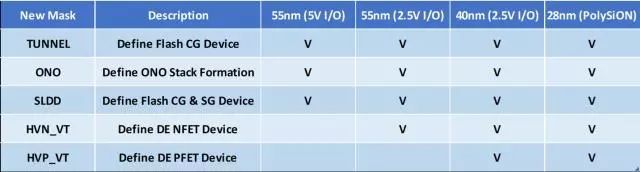
Lowest cost: Only 3~5 extra masks added into standard CMOS process.
-
Lowest power: 7.5V program/erase voltage, low-current FN/FN program/erase operations.
-
High Security: Resistant to decode by de-processing.
-
Ideal solution for consumer, industrial and especially IoT SoCs.
> MCU, Smart Card,EEPROM, FPGA, NOR Flash, etc.
Key SONOS Macro Specs
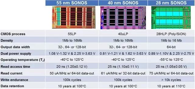
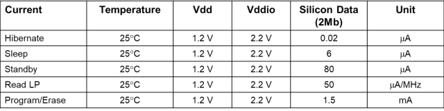
55 nm SONOS Macro Power Consumption
-
Balanced power consumption and performance (20ns Taa) for many applications
?Three power-saving modes: hibernate, sleep and standby.
?Low power read and program/erase operations to minimize active power.
?Low power read operation with Vdd=1.08 V to1.32 V.
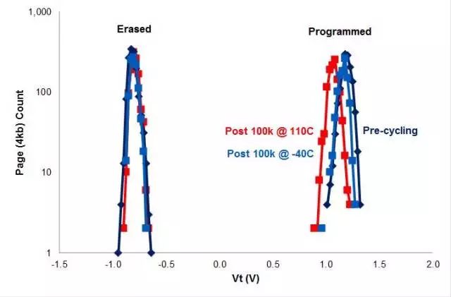
500hrs 225°C Yield w/ 50K Pre-cycling at 85 °C (55nm)
*All dies pass reading on full 8Mb after 500hrs 225°C bake
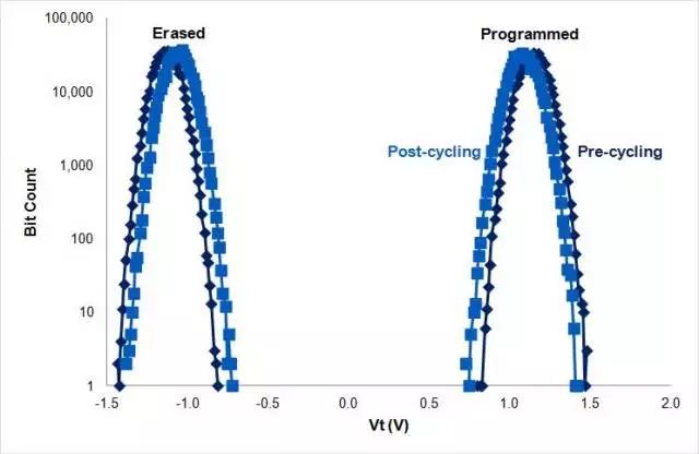
High Reliability
55-nm SONOS Macro Reliability
-
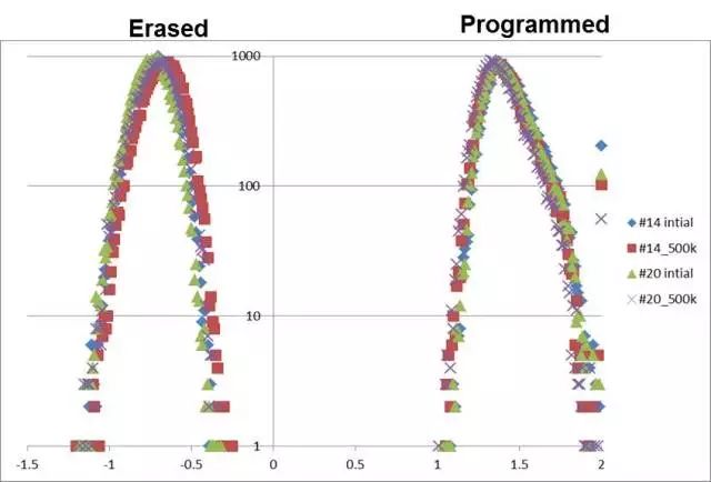
Endurance passes 500K cycles at 85°C w/o ECC. Vt window > 1.2V after 500K cycling.
-
Retention passes Automotive Grade-2 AEC Q100 requirement.
> Vt window > 0.6 V after 500 hrs bake @ 225C with 50K pre-cycling.
>滑动查看下一张图片<
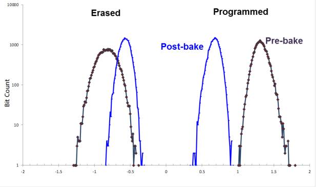
40-nm SONOS Macro Reliability
-
Endurance passes 500K cycles at 85°C w/o ECC. Vt window > 1.2V after 500K cycling.
-
Retention passes Automotive Grade-2 AEC Q100 requirement
>Vt window > 0.6 V after 500 hrs bake @ 225C with 50K pre-cycling.
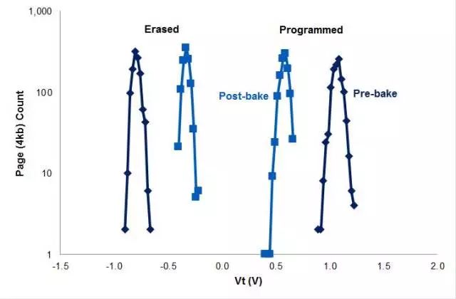
>滑动查看下一张图片<
28-nm SONOS Macro Reliability
-
Endurance passes 10K cycles at 125°C, Vt window >1.4 V after cycling.
-
Retention passes accelerated 48-hour bake at 250°C with > 0.7 V window left.
>滑动查看下一张图片<
55nm SONOS in Production Press Release
Customers NPI Status @ HLMC 55nm SONOS
-
Engaged > 15 customers.
-
7 Customers signed contract to use
-
3 in mass production
-
> 1,000 wafers started per month
SONOS eNVM Technology Availability
SONOS eNVM is scalable and proven in volume production on many nodes.
eCT Introduction
embedded Charge Trap
-
Based on charge-trap technology proven in six generations of MirrorBit? NOR Flash memory
Ideal solution for high-performance automotive MCUs
-
Fast 8 ns random access time from -40°C to 150°C junction temperature and 30 ms word programming speed
-
Smallest eNVM bit cell in the industry, 0.053 sq. ?m, at 40 nm node
-
Automotive Grade-1 reliability
Applications
-
Hybrid and electric vehicle motor control, instrument clusters, body control modules and HVAC
-
In volume production on UMC 40LP process flow
Key eCT Macro Specs
eCTReliability:
Automotive Qualification Data
-
Passed accelerated stress tests for Automotive Grade-1 per AEC-Q100 standard
40nm eCT in Production Press Release
Embedded NVM Solutions for Various Applications
Conclusion
Cypress develops and licenses charge-trap NVM technologies and Flash macro IP
-
Charge-trap NVMs serve in a wide range ofembedded applications
?SONOS: Consumer, Industrial SoCs
?eCT: high-performance automotive MCUs,Automotive Grade-1 reliability
-
Technologies are scalable to advanced nodes
?SONOS in mass production from 0.35um to 55nm, engineering samples available on 40uLP & 28HLP
?eCT is in volume production on UMC 40LP process
-
Low power for IoT: 0.9 V (40nm) or 1.2V(55nm) power supply, low-current operation, power-saving modes
-
Cost-effective: 3~5 (SONOS) or 8 (eCT)extra masks beyond the standard CMOS.
-
赛普拉斯
+关注
关注
28文章
393浏览量
88252 -
低功耗
+关注
关注
12文章
2829浏览量
105090
原文标题:赛普拉斯低成本高可靠嵌入式闪存技术
文章出处:【微信号:CypressChina,微信公众号:Cypress教程】欢迎添加关注!文章转载请注明出处。
发布评论请先 登录
【技术指南】提升嵌入式数据可靠性,从元器件选型开始!

赛普拉斯FRAM宽温域生命守护?
Linux嵌入式和单片机嵌入式的区别?
飞凌嵌入式即将受邀参加「菲尼克斯电气SoftPLC vPLC技术研讨会」
高可靠性嵌入式主板设计


 工商网监
工商网监
评论